News
SLC vs MLC: Proper Flash Selection for SSDs in Industrial, Military and Avionic Applications
Introduction
As with most storage technologies, NAND Flash vendors are constantly being pushed to reduce cost and increase density. One way the industry has responded is by packing more than one bit in a single flash storage cell. Known as Multi-Level Cell or MLC, this technology allows for a doubling or tripling of the data density with just a small increase in the cost and size of the overall silicon. But, this increase in density and decrease in cost per bit does come with its own tradeoffs. This paper will examine those tradeoffs, with an emphasis on how they affect the reliability of storage targeted at industrial, military and avionic applications.
These applications have very different demands from consumer applications, such as USB thumb drives, memory cards for digital cameras or even SSDs for consumer laptops or tablets. The environmental stresses, data endurance requirements and expected usable life of the products are much higher for industrial, military and avionic applications.
Flash Cell Operation
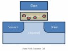
It is important to understand what makes up a Flash cell before discussing the differences between SLC and MLC NAND Flash. Each cell consists of a single transistor, with an additional “floating” gate that can store electrons. The diagram below shows the architecture of a basic Flash cell.
This operates as follows. For reading, the gate is electrically disconnected. The conductivity between the source and drain is then a function of the amount of charge on the floating gate. A voltage difference is set up between the drain and the source, V d – V s and is varied to determine the threshold voltage V t when current flows between source and drain. The threshold voltage represents the amount of charge on the gate. A large amount of charge is used to represent logic ‘0,’ and a small amount of charge used to represent logic ‘1’.
Writing is done by applying the programming voltage V p to the gate and grounding the channel, which sets up an electric field such that electrons are attracted to the surface of the channel. Some of these collide or encounter this barrier with enough energy to tunnel through the insulating layer. These are captured by the floating gate. Erasing is the opposite operation, with the gate grounded and with V p applied to the channel creating an electric field with the opposite polarity. This attracts electrons back to the channel, many of which will have enough energy to cross the insulating barrier. This process is called Fowler-Nordheim Tunneling.
This explains one of the key negatives of Flash technology. While it’s easy to attract electrons to the floating gate one cell at a time, it’s difficult to get them leave. Reversing the process requires putting the channel at a voltage which could disturb adjacent cells, since the channel is common to many cells. For this reason, Flash is erased in blocks, not a word or bit at a time. The blocks are sized by the Flash manufacturer in order to balance silicon area (since each erase block carries a fair amount of overhead circuitry) and ease of use. Because of the logic structure of NAND Flash, the Flash must also be written or read in fairly large pages (typically 1K to 4KB). These pages are written from or read to a page buffer, from which individual byte reads or writes are done. Each erase block contains between 32 and 128 pages.
This also helps explain why flash cells can only be written a limited number of times before they wear out. While many of the electrons travel with enough energy to cross the insulating oxide, some have enough to cross the barrier between the channel and oxide, but not enough to go all the way to the floating gate. These get trapped in the oxide. With each write/erase cycle, more electrons get trapped, which reduces the conductivity difference between the “programmed” and “erased” states. We will discuss this further when we talk about the endurance differences between SLC and MLC.
Single-Level Cell (SLC) Operation
SLC NAND Flash cells operate pretty much as described in the basic operation above. Both writing and erasing are done gradually to avoid over-stressing, which can degrade the lifetime of the cell by increasing the number of electrons trapped in the oxide or by causing oxide damage. Essentially, a write or erase is attempted, then stopped, and the cell is tested to see if the erase/write was successful. If not, it is reattempted, possibly with stronger or longer pulses. This is done several times until the operation time exceeds the specification and the cell is declared “bad.”
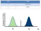
Since there are only two states, a cell represents only one bit value. Each bit can have a value of “programmed” or “erased.” A “0” or “1” is determined by the threshold voltage V t of the cell. The threshold voltage can be manipulated by the amount of charge put on the floating gate of the Flash cell. Placing a charge on the floating gate will increase the threshold voltage of the cell. When the threshold voltage is high enough, the cell will be read as programmed. No charge or threshold voltage of less than the minimum programmed voltage will cause the cell to be sensed as erased. As the cell wears, these two distributions move closer together, narrowing the difference between the values of V t for erased and programmed. When they overlap, it is impossible to distinguish between programmed and erased states.
2-Bit per Cell Multi-Level Cell (MLC)
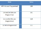
It is also possible to store more than one bit at each cell location by using multiple threshold voltages to encode multiple states. For example, the following state table could describe the amount of charge in the floating gate of the flash cell.
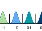
These four states yield two bits of information. After block erasure, the cell would be in the fully erased state. By increasing the number of electrons stored on the floating gate, the cell can be brought from fully erased to partially erased, to partially programmed and finally to fully programmed. This is done in the same manner as described earlier for gradually programming the SLC cell, by applying write pulses, then sensing the amount of charge to ensure that the cell was properly programmed.
As you can see in the figure, the gaps between the various states are much smaller than the gap between the two states of an SLC NAND Flash. Another way to describe this is that the signal-to-noise ratio of an MLC cell is much less than an SLC cell. Because of this, a more powerful error correction code is needed to correct for errors made due to noise, which can be either true electrical noise or “noise” induced by a trapped charge in a cell that has seen many program/erase cycles.
3-Bit Multi-Level Cell (MLC) Flash
The MLC concept can be extended beyond just 2 bits; 3 bits per cell (which is referred to by many as Three-Level Cell or TLC) is currently commercially available. Three bits actually yields 2 3 or eight levels as shown in the Table below. Some companies have begun to refer to 3 bits per cell as MLC-3, which is a better way to characterize it.
At this point, the difference in charge stored on the floating gate between the levels is on the order of 100 electrons or less, so for the time being, TLC is the practical limit of extending this concept (although there are companies beginning to experiment with 4 bits per cell). In fact, SanDisk has recently announced a 4 bit per cell NAND Flash for USB thumb drives. All of the issues with 2 bits per cell become even more difficult with a greater numbers of bits.
Which Technology for Industrial Use?
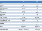
Now that the differences between MLC and SLC have been explained, let’s compare their specifications to make further distinctions between the two grades with an eye toward the requirements of military, avionics and industrial applications. These applications have more stringent demands on temperature range and the reliability of the storage. The cost of lost data in a critical mission is much higher than in consumer use. When life and property are on the line, or when you only get one shot at success, reliability is everything.
Performance
Since the same basic Flash cell is used for SLC and MLC NAND Flash, MLC can more than double the density with almost no die size penalty, and hence no manufacturing cost penalty (other than possibly yield loss). In fact, because of the large consumer demand for MLC NAND Flash for digital cameras, tablets and smart mobile phones, MLC enjoys economies of scale that allow it to cost less than half the cost per bit of SLC. The read bandwidths between SLC and MLC are comparable. SLC can read a 1KB page in about half the time that MLC can read a 2KB page. In general, the available bandwidth of a solid-state drive is more related to the controller architecture and design than to the speed of the Flash. However, the MLC NAND Flash technology does pay a price in terms of access speed. Access and programming times are two to three times slower than for the singlelevel design. But, for many consumer applications, this speed difference will be virtually undetectable.
Endurance
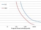
The endurance of SLC NAND Flash is 10 to 30 times more than MLC NAND Flash. This, and the operating temperature difference are the main reason why SLC NAND Flash is considered industrial-grade, and MLC NAND Flash is considered consumer-grade. The endurance difference is also generally not a problem in consumer use. For example, a USB drive application that used the 10,000 write/erase cycles would enable the user to completely write and erase the entire contents once per day for 27 years – m well beyond the life of the hardware. On the other hand, a data logging application that was constantly writing telemetry or sensor data might completely write the contents of the drive 10 times a day, leading to an endurance of only 2.7 years.
Error Rate
The error rate for MLC NAND Flash is 10 to 100 times worse than that of SLC NAND Flash and degrades more rapidly with increasing program/ erase cycles. This is driven by the very narrow margin between voltage threshold levels in MLC. There are 4 principal error mechanisms that affect Flash data reliability:
1. Program Disturb
2. Read Disturb
3. Leakage
4. Charge Trapping
Program disturb is caused by the stress to unselected cells in the same erase block as the cell being programmed. These unselected cells can either be adjacent bits on the same page, or the corresponding bit on adjacent pages. This voltage stress can cause a small amount of charge to be deposited on the floating gates of these adjoining cells, weakly programming them. While not a major problem for SLC NAND Flash, the addition of a small amount of charge can cause a shift between the levels in an MLC NAND Flash cell. This can be a particular problem with repeated program cycles of adjoining cells. For this reason, well-designed Flash controllers program pages sequentially within an erase block, and it’s also why MLC NAND Flash cannot withstand multiple writes per page.
Read disturb is caused by the voltage difference between the selected page being read and adjacent, unselected pages. This can stress the cells in the adjacent pages and cause a small amount of charge to be transferred to the gate of an erased cell, weakly programming them (again, this is a larger problem for MLC NAND Flash cells, since a very small voltage shift can affect the value stored).
Leakage of the charge on the floating gate is the phenomenon which leads to a limit on the data retention time for a cell. The floating gates can lose electrons at a very slow rate, on the order of an electron every week to every month. But, with the various values in multi-level cells only differentiated by 10s to 100s of electrons, this can lead to data retention times that are measured in months, rather than years. This is one of the reasons for the large difference between SLC and MLC data retention and endurance. Leakage is also increased by higher temperatures, which is why MLC NAND Flash is generally only appropriate for commercial temperature range applications.
The three previous error mechanisms are transient in nature. They only affect the reliability of the data stored in the cell and cause no physical change to the hardware of the flash cell. An erase and program of the cell will remove the error (another way to say this is that these data errors can be scrubbed).
The fourth error mechanism – charge trapping – does cause a permanent change to the cell. With every program or erase cycle, electrons which don’t quite have enough energy can get trapped in the insulating oxide between the channel and the floating gate. These electrons cause a permanent shift in the voltage threshold and narrow the gap between the erased and programmed states. They also interfere with the Fowler-Nordheim tunneling effect, which is the mechanism for moving electrons to and from the floating gate, and leads to longer program and erase times. At the end of a cell’s endurance, the programming or erase time becomes too long, and the page or block must be retired.
Conclusion
While MLC NAND Flash has definite advantages in the area of cost, SLC NAND Flash is a clear winner for rugged avionic, military and industrial applications. MLC NAND Flash issues with data retention at higher temperature, higher bit error rates and slower access times make it unsuitable for these applications. When human lives, critical missions or valuable capital are at stake, why trust anything less than the most reliable non-volatile storage available?
TCS Space & Component Technology specializes in high reliability, ruggedized solid state drives for the most demanding environments. With 35 years of industry experience, our team has the knowledge and expertise to provide engineering, manufacturing, quality, and technical services for military, space, and high reliability industrial customers.
If you’d like to know more information about the differences between SLC and MLC Flash, contact us!
(310) 214-5500 sctsales@telecomsys.com


